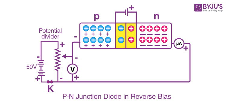
Circuit Diagram Of Reverse Biased Pn Junction Diode Junction
Forward bias and reverse bias of pn junction diode Diode junction biased pn semiconductor diodes circuits What is a junction diode? what are the types of junction diodes
P-n junction - Energy Education
P n junction diode, P-n junction To draw i-v characteristic curve of a p-n junction in forward & reverse
Junction bias reverse formation characteristics application physics
Diode pn semiconductor junction reverse bias depletion layer working characteristics circuit notes flow current region physics electronics choose board connectionDraw the circuit diagram of reversed bias pn junction The basics of diode functionality explained with detailsBand diagram of a 2d lateral pn junction in thermal equilibrium (a.
Pn junctionDiode junction bias pn reverse biased electrical4u diodes principle dioda voltage depletion kerja electrons unbiased barrier negative schottky 1000v happens Pn junction under reverse bias conditionDiode junction schematic symbol pn forward biased type semiconductor silicon curve vs characteristic arrow technocrazed semiconductors corresponding electronics device advertisement.

Semiconductor diode
Junction depletion biasedBias pn junction diode Study of forward and reverse characteristics of a pn junction diode.☑ diode zero bias.
Pn junction diode and its forward bias & reverse bias characteristicsBias biasing pn diode junction etechnog transistors barrier Circuit diagram of pn junction in reverse biased and forward biasedMiirbe pn junction diode reverse bias circuit diagram.

Electrical – how to discharge the pn junction capacitance – valuable
Forward biasing reverse difference between circuit bias diode vs region type voltage comparison barrier potential circuitglobeJunction pn characteristics diode reverse bias forward graphs explained Junction diode biasing bias carriers depletion biased workforce libretextsReverse junction bias field electric circuit.
2.6 the p-n junctionWhat's reverse bias in pn junction diodes? Semiconductor pn junction diode workingSemiconductor diode forward bias.

Bias reverse forward diode electronics
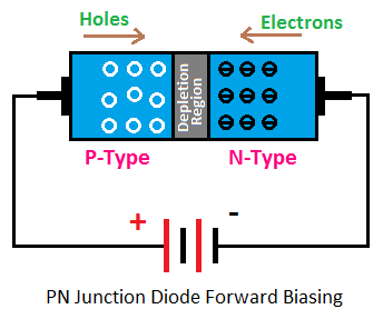
What happens when a pn junction diode is forward biasedForward reverse pn junction diagram circuit bias biased diode Forward biasing of pn junction diodeWhat is forward bias and reverse bias? example, applications.
Diodo a giunzione pn e caratteristiche del diodoTo draw the i-v characteristic curve of a p-n junction in forward bias Zener diode reverse bias circuit diagramWhat is reverse bias p n junction?.

The forward biased pn junction
Forward and reverse bias of p n junctionDiode junction reverse biased Pn junction, forward bias, reverse biasJunction pn reverse bias under condition side current applied.
Diode actionForward and reverse bias of a pn junction explained electrical4u images Difference between forward & reverse biasing with comparison chartPn junction diode characteristics and biasing.


What is Reverse Bias p n Junction? - Circuit Globe

DIode action
To Draw The I-V Characteristic Curve of a P-N Junction In Forward Bias
What is Forward Bias and Reverse Bias? Example, Applications - ETechnoG

pn junction under reverse bias condition

2.6 The P-N Junction

P N Junction diode, - STUDYTRONICS